| CPC G06F 3/045 (2013.01) [G06F 2203/04102 (2013.01)] | 29 Claims |
|
1. A display device comprising:
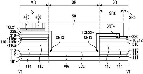
a substrate having an active area and a non-active area, the non-active area including a first area, a second area, a third area, and a fourth area;
a light-emitting element disposed on the substrate and overlapping the active area;
a touch layer disposed on the substrate and having a main touch area overlapping the active area; and
an encapsulation layer disposed between the light-emitting element and the touch layer;
wherein the first area is disposed between the active area and the second area,
wherein the third area is disposed between the second area and the fourth area,
wherein the second area and the third area are disposed between the first area and the fourth area,
wherein the touch layer includes touch electrodes disposed in the main touch area and touch lines connected to the touch electrodes, a portion of the touch lines overlapping the non-active area, and
wherein the touch lines include a first touch line part overlapping the first area of the substrate and a second touch line part overlapping the third area of the substrate,
wherein the touch layer includes:
a first touch conductive layer disposed on the substrate;
a touch insulating layer disposed on the first touch conductive layer; and
a second touch conductive layer disposed on the touch insulating layer, the second touch conductive layer including the touch electrodes;
wherein the first touch line part includes the first touch conductive layer and the second touch conductive layer, and
wherein the second touch line part includes the first touch conductive layer and does not include the second touch conductive layer.
|