| CPC G06F 3/0446 (2019.05) [G06F 1/1626 (2013.01); G06F 1/1637 (2013.01); G06F 1/1641 (2013.01); G06F 1/1643 (2013.01); G06F 1/1677 (2013.01); G06F 3/0412 (2013.01); G06F 3/1431 (2013.01); G06F 3/1446 (2013.01); G09G 2300/0426 (2013.01); G09G 2330/04 (2013.01); G09G 2340/0442 (2013.01); G09G 2354/00 (2013.01); G09G 2380/02 (2013.01)] | 6 Claims |

|
1. A data processing device comprising:
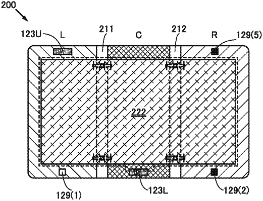
a display portion being foldable and having a first region, a second region being adjacent to the first region, and a third region being adjacent to the second region,
wherein each of the first region, the second region, and the third region comprises a light-emitting element,
wherein when the display portion is folded to face inward, a part of the display portion which does not face a user of the data processing device is configured to stop displaying,
wherein the part of the display portion includes at least the second region,
wherein the display portion comprises:
a first substrate having flexibility;
a first adhesive layer over the first substrate;
a transistor over the first adhesive layer;
an insulating layer over the transistor;
a lower electrode of a light-emitting element over the insulating layer;
a partition having a region overlapping with a first part of the lower electrode;
a layer containing a light-emitting organic compound, the layer overlapping with a second part of the lower electrode;
an upper electrode of the light-emitting element over the layer;
a photodiode below the light-emitting element;
a coloring layer over the upper electrode;
a second adhesive layer over the coloring layer; and
a second substrate having flexibility, and
wherein the photodiode is not overlapped with the light-emitting element, the partition, and the coloring layer.
|