| CPC G06F 13/1689 (2013.01) [G06F 1/04 (2013.01); G06F 1/06 (2013.01); G06F 1/08 (2013.01); G06F 1/10 (2013.01); G06F 13/161 (2013.01); G06F 13/1657 (2013.01); G11C 7/222 (2013.01); G11C 7/04 (2013.01); H04L 7/033 (2013.01)] | 20 Claims |
|
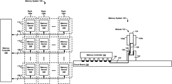
1. A memory controller to control the operation of first and second memory devices configured as respective first and second ranks, the memory controller comprising:
a strobe receiver circuit to receive, via a strobe signal line:
a first strobe signal from the first memory device, wherein the first memory device is configured in a first rank of memory; and
a second strobe signal from the second memory device, wherein the second memory device is configured in a second rank of memory;
a calibration circuit operable in a calibration mode to generate rank specific calibration data for the first memory device and the second memory device, the calibration data including:
first calibration data based on the first strobe signal received from the first memory device via the strobe signal line; and
second calibration data based on the second strobe signal received from the second memory device via the strobe signal line;
and
a data sampling circuit, to receive:
first read data in association with read operations from the first memory device, the first read data to be received using an adjusted sampling phase based on the first calibration data; and
second read data in association with read operations from the second memory device, the second read data to be received using an adjusted sampling phase based on the second calibration data.
|