| CPC G06F 12/023 (2013.01) [G06F 2212/1008 (2013.01)] | 19 Claims |
|
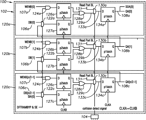
1. A circuit comprising:
comparator circuitry coupled to peripheral circuitry to a multiport memory, wherein the comparator circuitry is configured to transmit one or more data input signals or one or more write enable signals from respective inputs of the peripheral circuitry to respective memory outputs when a memory address collision is detected for one or more respective bitcells of the multi-port memory, wherein the peripheral circuitry comprises one or more data input sections, wherein:
for each data input section:
a first multiplexer is configured to receive a data input signal;
an AND gate is configured to receive a write enable signal; and
first and second latches are configured to receive the data input signal and the write enable signal and output the respective signals to an OR gate.
|