| CPC G06F 1/10 (2013.01) [G06F 1/12 (2013.01); G06F 11/0733 (2013.01); G06F 11/0751 (2013.01); G06F 11/0772 (2013.01); G06F 11/0793 (2013.01)] | 12 Claims |
|
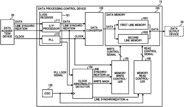
1. A data processing control device comprising:
a data receiver configured to receive data to be processed, an external clock generated externally from the data processing control device, and a unit control signal determining a processing unit as an amount of the data to be processed, the data receiver including a phase locked loop (PLL) circuit configured to receive the external clock;
a clock abnormality detector configured to receive a lock signal output from the PLL circuit and the unit control signal and operate based on a clock different from the external clock and output a write synchronization signal, a read synchronization signal and a write mask signal based on the lock signal and the unit control signal;
a memory write controller configured to produce a write control signal based on the write synchronization signal and the write mask signal;
a memory read controller configured to produce a read control signal based on the read synchronization signal; and
a first memory and a second memory configured to alternatively write and read the data to be processed based on the write control signal and the read control signal,
wherein when abnormality of the external clock occurs, the memory write controller produces the write control signal to stop writing of the data to be processed in the first memory or the second memory, and
when the external clock becomes normal again, to take in the unit control signal, the memory write controller produces the write control signal to write the data to be processed in the first memory or the second memory.
|