| CPC G05F 1/56 (2013.01) [G11C 5/147 (2013.01); G11C 7/10 (2013.01); H03F 3/45071 (2013.01)] | 20 Claims |

|
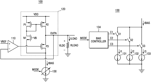
1. A semiconductor device comprising:
an error amplifier configured to receive a voltage of an output node and a reference voltage;
a flipped voltage follower (FVF) circuit configured to receive an output of the error amplifier and maintain the voltage of the output node at the reference voltage; and
a bias current control circuit configured to
receive a first mode signal, a second mode signal, and a third mode signal,
control a magnitude of a bias current flowing through the FVF circuit based on the first mode signal, the second mode signal, and the third mode signal,
control the bias current of a first magnitude to flow through the FVF circuit, in response to the first mode signal,
control the bias current of a second magnitude smaller than the first magnitude to flow through the FVF circuit, in response to the second mode signal, and
control the bias current of a third magnitude smaller than the second magnitude to flow through the FVF circuit, in response to the third mode signal.
|