| CPC G03G 15/80 (2013.01) [G03G 15/0863 (2013.01); G03G 21/1652 (2013.01); G03G 21/1803 (2013.01); G03G 21/1867 (2013.01); G03G 21/1885 (2013.01); G03G 15/0216 (2013.01); G03G 15/087 (2013.01); G03G 15/5008 (2013.01); G03G 21/1846 (2013.01); G03G 2215/00713 (2013.01); G03G 2215/0872 (2013.01)] | 12 Claims |
|
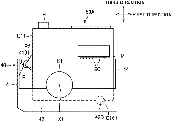
1. A process cartridge comprising:
a development roller rotatable about a first axis extending in a first direction;
a photosensitive drum;
a frame having a first outer surface and a second outer surface spaced apart from the first outer surface in the first direction,
a drum coupling rotatable with the photosensitive drum, the drum coupling positioned at the first outer surface in the first direction,
a first electrode positioned at the second outer surface, the first electrode including a first electrical contact surface facing outward in the first direction;
a second electrode positioned at the second outer surface, the second electrode including a second electrical contact surface facing outward in the first direction;
a third electrode positioned at the second outer surface, the third electrode including a third electrical contact surface facing outward in the first direction; and
a fourth electrode positioned at the second outer surface, the fourth electrode including a fourth electrical contact surface facing outward in the first direction; and
a memory positioned at the second outer surface, the memory including a memory contact surface facing outward in the first direction,
wherein the first electrical contact surface, the second electrical contact surface, the third electrical contact surface, the fourth electrical contact surface and the memory contact surface are spaced away from each other at the second outer surface.
|