| CPC G03F 7/7065 (2013.01) [G03F 7/702 (2013.01); G03F 7/70625 (2013.01); H01L 21/0274 (2013.01)] | 45 Claims |

|
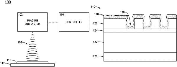
19. A characterization system comprising:
an imaging sub-system configured to acquire image data from a semiconductor stack including one or more layers, wherein the semiconductor stack includes a metal layer of at least one of molybdenum, nickel, tungsten, rhodium, vanadium, or palladium having a thickness between 0.5 and 10 nm deposited on a layer of the semiconductor stack to form a reflective surface on the layer, wherein a thickness of the metal layer on a side-wall of one or more patterns of the one or more layers of the semiconductor stack is less than a thickness of the metal layer on a top of one or more patterns of the one or more layers of the semiconductor stack;
a controller communicatively coupled to the imaging sub-system, the controller including one or more processors configured to execute program instructions causing the one or more processors to:
receive image data of the reflective surface on the layer of the semiconductor stack from the imaging sub-system; and
identify one or more gap defects within the layer based on illumination reflected from the reflective surface.
|