| CPC G03F 7/70633 (2013.01) [G02B 6/1225 (2013.01); G02B 26/0833 (2013.01)] | 20 Claims |
|
1. A sensor apparatus comprising:
a sensor chip comprising a first side and a second side opposite the first side;
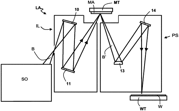
an illumination system coupled to the sensor chip and configured to transmit an illumination beam along an illumination path;
a first optical system disposed on the sensor chip and comprising a first integrated optic configuration to configure and transmit the illumination beam toward a diffraction target on a substrate, disposed adjacent to the sensor chip, and generate a signal beam comprising diffraction order sub-beams generated from the diffraction target;
a second optical system disposed on the sensor chip and comprising a second integrated optic configuration to collect and transmit the signal beam from the first side to the second side of the sensor chip; and
a detector system configured to measure a characteristic of the diffraction target based on the signal beam transmitted by the second optical system.
|