US 12,066,757 B2
Mask and method of forming the same
Chih-Chiang Tu, Tauyen (TW); Chun-Lang Chen, Tainan (TW); Shih-Hao Yang, Tainan (TW); and Jheng-Yuan Chen, Hsinchu (TW)
Assigned to Taiwan Semiconductor Manufacturing Company, Ltd., Hsinchu (TW)
Filed by Taiwan Semiconductor Manufacturing Company, Ltd., Hsinchu (TW)
Filed on Apr. 27, 2023, as Appl. No. 18/308,635.
Application 18/308,635 is a continuation of application No. 17/100,970, filed on Nov. 23, 2020, granted, now 11,662,656.
Application 17/100,970 is a continuation of application No. 15/992,203, filed on May 30, 2018, granted, now 10,845,698, issued on Nov. 24, 2020.
Prior Publication US 2023/0259014 A1, Aug. 17, 2023
This patent is subject to a terminal disclaimer.
Int. Cl. G03F 1/54 (2012.01); G03F 1/22 (2012.01); G03F 1/24 (2012.01); G03F 1/26 (2012.01); G03F 1/52 (2012.01); G03F 1/80 (2012.01); H01L 21/033 (2006.01)
CPC G03F 1/26 (2013.01) [G03F 1/22 (2013.01); G03F 1/24 (2013.01); G03F 1/52 (2013.01); G03F 1/54 (2013.01); G03F 1/80 (2013.01); H01L 21/0337 (2013.01)] 20 Claims
OG exemplary drawing
 
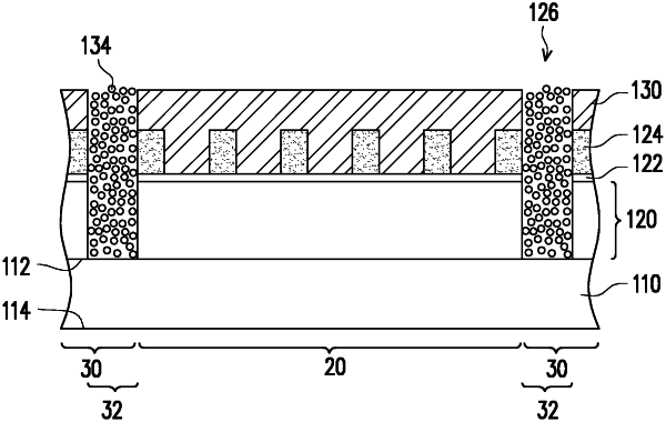
1. A mask, comprising:
a reflective layer;
an absorption layer over the reflective multilayer;
an absorption part, disposed in the reflective layer and the absorption layer, wherein an entire top surface of the absorption part is substantially flush with a top surface of the absorption layer; and
a buffer layer, disposed between the reflective layer and the absorption layer, wherein the absorption part is further disposed in the buffer layer.