| CPC G02F 1/294 (2021.01) [G02F 2202/30 (2013.01); G02F 2202/36 (2013.01); G02F 2203/50 (2013.01); H04N 23/67 (2023.01)] | 24 Claims |

|
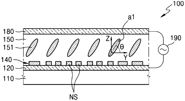
1. A meta-optical device which imparts a phase delay to incident light of a wavelength band, the meta-optical device comprising:
a first electrode and a second electrode spaced apart from each other;
a liquid crystal layer between the first electrode and the second electrode;
a meta-surface layer located within the liquid crystal layer, the meta-surface layer comprising a plurality of nanostructures each having a shape dimension smaller than a center wavelength of the wavelength band; and
a voltage device configured to apply a voltage between the first electrode and the second electrode,
wherein the meta-surface layer comprises a plurality of unit cells, and
wherein each of the plurality of unit cells comprises a pair of a first nanostructure of the plurality of nanostructures and a second nanostructure of the plurality of nanostructures, wherein the first nanostructure has different dimensions from the second nanostructure.
|