| CPC G02F 1/155 (2013.01) [G02F 1/134336 (2013.01); G02F 2201/123 (2013.01); H10K 59/131 (2023.02)] | 22 Claims |

|
1. A display device, comprising:
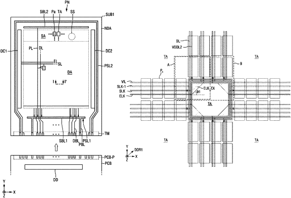
a substrate comprising a display area comprising a plurality of main pixels, and a sensor area comprising a plurality of auxiliary pixels and a plurality of transmission portions; and
a plurality of wirings arranged along edges of the plurality of transmission portions and electrically connecting the plurality of auxiliary pixels,
wherein:
the plurality of wrings comprises a plurality of first directional wirings extending in a first direction and arranged with each other in a second direction crossing the first direction, and a plurality of second directional wirings extending in the second direction and arranged with each other in the first direction, and
a wiring adjacent to the transmission portion from among the plurality of first directional wirings comprises a first extension portion,
wherein the plurality of first directional wirings comprise a first wiring to apply an initialization voltage into auxiliary pixels arranged in the first direction from among the plurality of auxiliary pixels and a second wiring to apply a first scan signal into the auxiliary pixels arranged in the first direction, and
wherein in an area in which the auxiliary pixels arranged in the first direction are arranged, the second wiring is on the substrate, a first insulation layer is on the second wiring and the first wiring is on the first insulation layer.
|