US 12,066,730 B2
Liquid crystal display device
Shunpei Yamazaki, Setagaya (JP); Yukie Suzuki, Atsugi (JP); Hideaki Kuwabara, Isehara (JP); and Hajime Kimura, Atsugi (JP)
Assigned to Semiconductor Energy Laboratory Co., Ltd., Atsugi (JP)
Filed by Semiconductor Energy Laboratory Co., Ltd., Atsugi (JP)
Filed on Aug. 8, 2023, as Appl. No. 18/231,383.
Application 16/411,594 is a division of application No. 15/698,904, filed on Sep. 8, 2017, granted, now 10,338,447, issued on Jul. 2, 2019.
Application 18/231,383 is a continuation of application No. 17/537,958, filed on Nov. 30, 2021, granted, now 11,726,378.
Application 17/537,958 is a continuation of application No. 16/912,853, filed on Jun. 26, 2020, granted, now 11,194,207, issued on Dec. 7, 2021.
Application 16/912,853 is a continuation of application No. 16/726,444, filed on Dec. 24, 2019, granted, now 10,712,625, issued on Jul. 14, 2020.
Application 16/726,444 is a continuation of application No. 16/411,594, filed on May 14, 2019, granted, now 10,678,107, issued on Jun. 9, 2020.
Application 15/698,904 is a continuation of application No. 14/859,741, filed on Sep. 21, 2015, granted, now 9,766,526, issued on Sep. 19, 2017.
Application 14/859,741 is a continuation of application No. 14/489,990, filed on Sep. 18, 2014, granted, now 9,188,825, issued on Nov. 17, 2015.
Application 14/489,990 is a continuation of application No. 13/909,398, filed on Jun. 4, 2013, granted, now 8,842,230, issued on Sep. 23, 2014.
Application 13/909,398 is a continuation of application No. 13/681,880, filed on Nov. 20, 2012, granted, now 8,462,286, issued on Jun. 11, 2013.
Application 13/681,880 is a continuation of application No. 13/332,786, filed on Dec. 21, 2011, granted, now 8,325,285, issued on Dec. 4, 2012.
Application 13/332,786 is a continuation of application No. 12/795,040, filed on Jun. 7, 2010, granted, now 8,111,362, issued on Feb. 7, 2012.
Application 12/795,040 is a continuation of application No. 12/213,729, filed on Jun. 24, 2008, granted, now 7,738,050, issued on Jun. 15, 2010.
Claims priority of application No. 2007-179092 (JP), filed on Jul. 6, 2007.
Prior Publication US 2024/0027863 A1, Jan. 25, 2024
Int. Cl. G02F 1/1368 (2006.01); G02F 1/1333 (2006.01); G02F 1/1339 (2006.01); G02F 1/1343 (2006.01); G02F 1/1362 (2006.01); H01L 27/12 (2006.01); H01L 29/04 (2006.01); H01L 29/66 (2006.01); H01L 29/786 (2006.01); H01L 29/45 (2006.01); H01L 29/49 (2006.01)
CPC G02F 1/1368 (2013.01) [G02F 1/133345 (2013.01); G02F 1/1339 (2013.01); G02F 1/134309 (2013.01); G02F 1/136286 (2013.01); H01L 27/1214 (2013.01); H01L 27/1222 (2013.01); H01L 27/1288 (2013.01); H01L 29/04 (2013.01); H01L 29/66765 (2013.01); H01L 29/78678 (2013.01); H01L 29/78696 (2013.01); H01L 29/458 (2013.01); H01L 29/4908 (2013.01)] 15 Claims
OG exemplary drawing
 
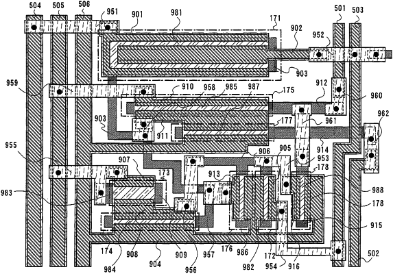
1. A display device comprising:
a first conductive layer having a function of a gate electrode of a transistor;
a first insulating layer over the first conductive layer;
a semiconductor layer over the first insulating layer, the semiconductor layer having a channel formation region of the transistor;
a second conductive layer over the semiconductor layer, the second conductive layer having a function of one of a source electrode and a drain electrode of the transistor;
a third conductive layer over the semiconductor layer, the third conductive layer having a function of the other of the source electrode and the drain electrode of the transistor;
a second insulating layer having a region in contact with a surface of the second conductive layer and a region in contact with a surface of the third conductive layer;
a fourth conductive layer over the second insulating layer, the fourth conductive layer having a function of a wiring; and
a pixel electrode over the second insulating layer,
wherein the second conductive layer is electrically connected to the fourth conductive layer through a first contact hole in the second insulating layer,
wherein the third conductive layer is electrically connected to the pixel electrode through a second contact hole in the second insulating layer,
wherein the fourth conductive layer has a stacked-layer structure,
wherein a thickness of the second conductive layer is smaller than a thickness of the fourth conductive layer, and
wherein an area of the second conductive layer overlapping with the semiconductor layer overlaps with the first conductive layer.