| CPC G02F 1/134345 (2021.01) [G02F 1/133512 (2013.01); G02F 1/133707 (2013.01); G02F 1/136209 (2013.01); G02F 1/136286 (2013.01); H01L 27/124 (2013.01); G02F 1/13439 (2013.01); G02F 1/1368 (2013.01)] | 16 Claims |
|
1. An array base plate, wherein the array base plate comprises a substrate and a plurality of sub-pixels that are provided on the substrate and are arranged in an array;
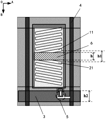
each of the sub-pixels comprises a first slit electrode and a second slit electrode that are arranged in a first direction;
the first slit electrode comprises a plurality of first slits that are arranged parallelly and separately, the second slit electrode comprises a plurality of second slits that are arranged parallelly and separately, and a direction of extension of the first slits and a direction of extension of the second slits are different; and
the sub-pixel further comprises a dark-area light shielding part located over the first slit electrode and the second slit electrode, and an orthographic projection of the dark-area light shielding part on the substrate at least partially covers an orthographic projection of a first area of the sub-pixel on the substrate, wherein the first area is an area between the first slit electrode and the second slit electrode;
wherein the array base plate further comprises a plurality of grid lines that are arranged in the first direction, and the grid lines are located between two adjacent rows of the sub-pixels in the first direction;
the sub-pixel further comprises a grid-line light shielding part, and the orthographic projection of the grid-line light shielding part on the substrate covers the orthographic projection of the grid line on the substrate;
wherein a width of the dark-area light shielding part in the first direction is less than or equal to one-half of a width of the grid-line light shielding part in the first direction; and
wherein the width of the dark-area light shielding part in the first direction is less than or equal to a maximum width of the first area in the first direction;
wherein in the sub-pixel, an included angle between the direction of extension of the first slits and a second direction is a first included angle, and an included angle between the direction of extension of the second slits and the second direction is a second included angle, wherein the second direction and the first direction are perpendicular; and
the maximum width of the first area in the first direction is correlated with the first included angle and the second included angle.
|