| CPC G02F 1/0121 (2013.01) [G02B 1/002 (2013.01); G02F 1/0018 (2013.01)] | 28 Claims |
|
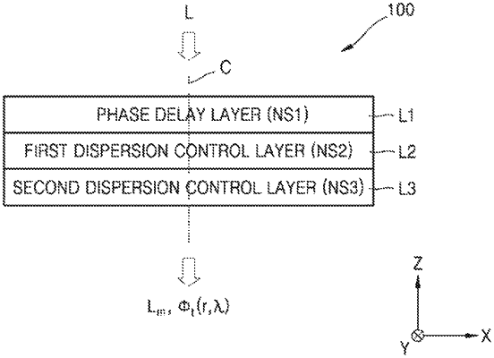
1. A meta-optical device which exhibits a target phase delay profile with respect to incident light in a predetermined wavelength band, the meta-optical device comprising:
a first layer including a plurality of first nanostructures and a first surrounding material surrounding the plurality of first nanostructures, the first layer having a first phase delay profile of a first tendency that is substantially equal to a tendency of the target phase delay profile;
a second layer provided adjacent to the first layer and including a plurality of second nanostructures and a second surrounding material surrounding the plurality of second nanostructures, the second layer having a second phase delay profile of a second tendency that is substantially opposite to the tendency of the target phase delay profile; and
a third layer provided adjacent to the second layer and including a plurality of third nanostructures and a third surrounding material surrounding the plurality of third nanostructures, the third layer having a third phase delay profile different from the second phase delay profile, wherein the third layer includes a third material that is different than a second material of the second layer, or includes a third arrangement rule that is different than a second arrangement rule of the second layer.
|