| CPC G02B 7/006 (2013.01) [G02B 13/00 (2013.01); H01L 31/0203 (2013.01); H01L 31/02325 (2013.01)] | 11 Claims |

|
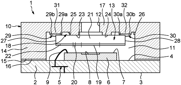
1. A method of fabricating an electronic device, comprising:
providing a carrier substrate having a front face to which at least one electronic chip is mounted;
providing an encapsulation cover having a front opening and, around the front opening, a back mounting face which comprises at least one contact area and at least one local cavity which is recessed with respect to the at least one contact area;
providing an optical element through which light is able to pass, wherein the optical element includes a central region designed to deviate the light and a positioning pattern;
mounting the optical element to the encapsulation cover at a position behind the front opening, wherein mounting the optical element comprises:
applying a drop of adhesive; and
positioning a face of the optical element in contact with the at least one contact area of the back mounting face;
wherein said drop of adhesive fixes the optical element to the back mounting face and extends locally into the at least one local cavity; and
mounting the encapsulation cover on top of the front face of the carrier substrate, in a position such that the electronic chip is situated within a chamber bounded by the encapsulation cover and that the optical element is in front of the optical component of the electronic chip;
wherein mounting the encapsulation cover further comprises:
placing the encapsulation cover equipped with the optical element in a reference position;
detecting the positioning pattern of the optical element through a back of the encapsulation cover with respect to a position of at least one of the carrier substrate and the electronic chip mounted on the carrier substrate; and
moving and mounting the encapsulation cover on top of the carrier substrate, starting from the reference position and according to a movement and mounting program.
|