| CPC G02B 6/4283 (2013.01) [G02B 6/4238 (2013.01); G02B 6/43 (2013.01)] | 20 Claims |
|
1. A semiconductor device, comprising:
a plurality of intermediate waveguides;
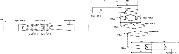
wherein the plurality of intermediate waveguides are vertically disposed on top of one another, and vertically adjacent ones of the plurality of intermediate waveguides are laterally offset from each other; and
wherein, when viewed from the top, each of the plurality of intermediate waveguides essentially consists of a first portion and a second portion, the first portion has a first varying width that increases from a first end of the corresponding intermediate waveguide to a middle of the corresponding intermediate waveguide, and the second portion has a second varying width that decreases from the middle of the corresponding intermediate waveguide to a second end of the corresponding intermediate waveguide.
|