| CPC G02B 6/12 (2013.01) [G02B 2006/12069 (2013.01); G02B 2006/12166 (2013.01)] | 18 Claims |
|
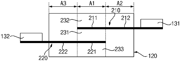
1. A graphene optical device comprising:
an upper semiconductor layer;
a lower semiconductor layer; and
a graphene capacitor disposed between the upper semiconductor layer and the lower semiconductor layer,
wherein the graphene capacitor comprises a first graphene, a second graphene, a first insulation layer disposed between the first graphene and the second graphene, a first graphene gate disposed between the first graphene and the upper semiconductor layer, and a second graphene gate disposed between the second graphene and the lower semiconductor layer, and
wherein the first graphene and the second graphene partially overlap each other when viewed from the upper semiconductor layer toward the lower semiconductor layer.
|