| CPC G02B 1/002 (2013.01) [G01B 11/24 (2013.01); G02B 5/1809 (2013.01); G02B 5/1871 (2013.01); G02B 2207/101 (2013.01)] | 38 Claims |
|
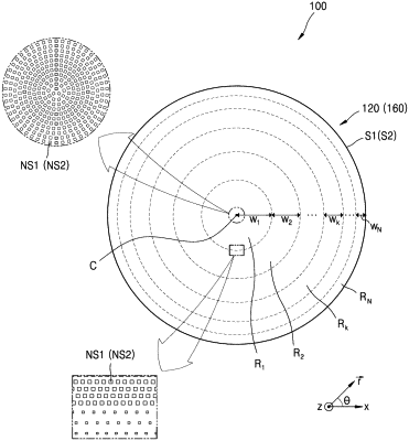
1. A meta-optical device comprising:
a first layer comprising a plurality of first nanostructures spaced apart from each other in a horizontal direction and a first material disposed adjacent to each first nanostructure of the plurality of first nanostructures;
a second layer disposed on the first layer in a vertical direction, the second layer comprising a plurality of second nanostructures spaced apart from each other in the horizontal direction and a second material disposed adjacent to each second nanostructure of the plurality of second nanostructures,
wherein the first layer and the second layer comprise regions in which signs of an effective refractive index change rate in a first direction are opposite to each other, and
wherein the meta-optical device is configured to obtain a target phase delay profile with respect to incident light of a predetermined wavelength band.
|