| CPC G01T 1/2018 (2013.01) [H01L 27/14605 (2013.01); H01L 27/14663 (2013.01); H01L 31/03926 (2013.01)] | 16 Claims |
|
1. A photodetection device, comprising:
a substrate;
a plurality of pixel units on the substrate, the plurality of pixel units being in a matrix of a row direction and a column direction;
a first photodetector included in a pixel unit of the plurality of pixel units, the pixel unit including the first photodetector being in an active area usable for photodetection on the substrate; and
a second photodetector included in a pixel unit of the plurality of pixel units, the pixel unit including the second photodetector being in an inactive area unusable for photodetection, the inactive area surrounding the active area on the substrate,
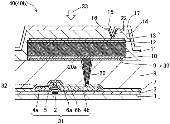
wherein the first photodetector includes
a first lower electrode layer on the substrate,
a first lower extrinsic semiconductor layer on the first lower electrode layer, the first lower extrinsic semiconductor layer being inside the first lower electrode layer in a plan view, the first lower extrinsic semiconductor layer comprising a first extrinsic semiconductor,
a first intrinsic semiconductor layer on the first lower extrinsic semiconductor layer,
a first upper extrinsic semiconductor layer on the first intrinsic semiconductor layer, the first upper extrinsic semiconductor layer comprising a second extrinsic semiconductor, and
a first upper electrode layer on the first upper extrinsic semiconductor layer, and
the second photodetector includes
a second lower electrode layer on the substrate,
a second lower extrinsic semiconductor layer on the second lower electrode layer, the second lower extrinsic semiconductor layer covering the second lower electrode layer, the second lower extrinsic semiconductor layer comprising the first extrinsic semiconductor,
a second intrinsic semiconductor layer on the second lower extrinsic semiconductor layer,
a second upper extrinsic semiconductor layer on the second intrinsic semiconductor layer, the second upper extrinsic semiconductor layer comprising the second extrinsic semiconductor, and
a second upper electrode layer on the second upper extrinsic semiconductor layer.
|