| CPC G01R 27/2605 (2013.01) [G01R 31/2639 (2013.01); G01R 31/2841 (2013.01); H03K 19/094 (2013.01)] | 19 Claims |

|
1. A method comprising:
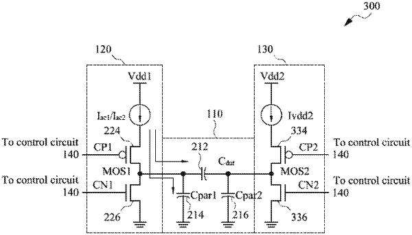
applying a first voltage to a first transistor of a first pseudo-inverter circuit and a second voltage to a second transistor of a second pseudo-inverter circuit, wherein a device under test is coupled between the first pseudo-inverter circuit and the second pseudo-inverter circuit, a third transistor is coupled between the first transistor and ground, and a fourth transistor is coupled between the second transistor and the ground; and
performing only two measurement steps, wherein:
during a first measurement step, the first and fourth transistors are turned on, the second and third transistors are turned off, and a first current, induced by a capacitance of the device under test and a parasitic capacitance, is measured; and
during a second measurement step, the first and second transistors are turned on, the third and fourth transistors are turned off, and a second current, induced by the parasitic capacitance, is measured, and wherein a capacitance (Cdut) of the device under test is expressed as follows:
 where Iac1 is the first current, Iac2 is the second current, Vdd1 is the first voltage, and f is a clock frequency.
|