| CPC G01N 27/9006 (2013.01) [B22F 5/12 (2013.01); B29C 64/153 (2017.08); G01N 29/041 (2013.01); B33Y 10/00 (2014.12); B33Y 80/00 (2014.12)] | 20 Claims |
|
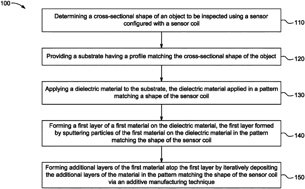
1. A method of manufacturing comprising:
determining a cross-sectional shape of an object to be inspected using a sensor configured with a sensor coil;
providing a substrate having a profile matching the cross-sectional shape of the object;
applying a dielectric material to the substrate, the dielectric material applied in a pattern matching a shape of the sensor coil;
forming a first layer of a first material on the dielectric material, the first layer formed by sputtering particles of the first material on the dielectric material in the pattern matching the shape of the sensor coil;
forming additional layers of the first material atop the first layer by iteratively depositing the additional layers of the first material in the pattern matching the shape of the sensor coil via an additive manufacturing technique.
|