US 12,066,329 B2
Sensor array spectrometer
John A. Wheatley, Stillwater, MN (US); Mark A. Roehrig, Stillwater, MN (US); Audrey A. Sherman, Woodbury, MN (US); Del R. Lawson, Cottage Grove, MN (US); Gilles J. Benoit, Minneapolis, MN (US); Daniel J. Schmidt, Woodbury, MN (US); Jonah Shaver, St. Paul, MN (US); Raymond J. Kenney, Woodbury, MN (US); and Zhaohui Yang, North Oaks, MN (US)
Assigned to 3M INNOVATIVE PROPERTIES COMPANY, St. Paul, MN (US)
Appl. No. 17/440,004
Filed by 3M INNOVATIVE PROPERTIES COMPANY, St. Paul, MN (US)
PCT Filed Mar. 19, 2020, PCT No. PCT/IB2020/052538
§ 371(c)(1), (2) Date Sep. 16, 2021,
PCT Pub. No. WO2020/194146, PCT Pub. Date Oct. 1, 2020.
Claims priority of provisional application 62/823,858, filed on Mar. 26, 2019.
Prior Publication US 2022/0178749 A1, Jun. 9, 2022
Int. Cl. G01J 3/28 (2006.01); G02B 5/22 (2006.01)
CPC G01J 3/2803 (2013.01) [G02B 5/22 (2013.01)] 15 Claims
OG exemplary drawing
 
1. An optical device, comprising:
an optical sensor;
a plurality of photosensitive pixels disposed on the optical sensor; and
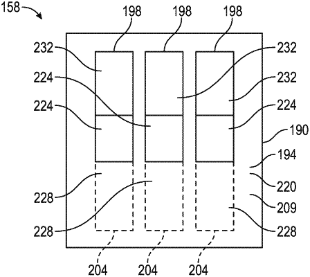
a wavelength-selective optical filter in optical communication with the photosensitive pixels, the wavelength-selective optical filter comprising first and second filter sheets, each of the first and second filter sheets defining therein a plurality of spatially-variant written regions and at least one non-written region, the written and non-written regions of the first and second filter sheets partially overlapping one another to define first through fourth areas of the optical filter having respective different first through fourth transmission spectra, each of the first through fourth areas being larger than each of the pixels.