| CPC C30B 29/40 (2013.01) [C30B 33/10 (2013.01); H01L 21/02021 (2013.01); H01L 21/304 (2013.01); H01L 29/20 (2013.01)] | 7 Claims |

|
1. An indium phosphide substrate,
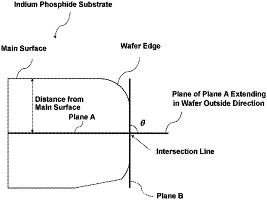
wherein when planes A each parallel to a main surface are taken in a wafer, the phosphide substrate has an angle θ on the main surface side of 0°<θ≤120° for all of the planes A where a distance from the main surface is 100 μm or more to 200 μm or less, wherein the angle θ is formed by a plane B, the plane B including an intersection line of an wafer edge with each of the planes A and being tangent to the wafer edge, and an plane of each of the planes A extending in a wafer outside direction;
wherein in a cross section orthogonal to the wafer edge, the indium phosphide substrate has edge rounds on the main surface side and a surface side opposite to the main surface;
wherein a chamfered width Xf from the wafer edge on the main surface side is 50 μm or more to 130 μm or less;
wherein a chamfered width Xb from the wafer edge on the surface side opposite to the main surface is 150 μm or more to 400 μm or less; and
wherein the indium phosphide substrate has a thickness of 330 μm or more to 700 μm or less.
|