| CPC H10N 10/852 (2023.02) [C01B 19/04 (2013.01); G01J 5/12 (2013.01); H10N 10/857 (2023.02)] | 14 Claims |
|
14. A thermoelectric conversion material comprising:
a base material that is a semiconductor composed of a base material element;
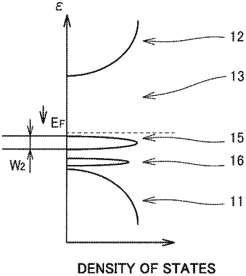
a first additional element, the first additional element being an element different from the base material element, the first additional element having a vacant orbital in a d orbital or f orbital located internal to an outermost shell of the first additional element, the first additional element forming a first additional level in a forbidden band of the base material; and
a second additional element, the second additional element being an element different from both of the base material element and the first additional element, the second additional element forming a second additional level in the forbidden band of the base material, wherein
a difference is 1 between the number of electrons in an outermost shell of the second additional element and the number of electrons in at least one outermost shell of the base material element,
wherein a crystal phase having a grain size of less than or equal to 50 nm and composed of the base material element is included in a structure of the thermoelectric conversion material,
wherein a ratio of an intensity of a peak having a maximum intensity in peaks each indicating a crystal phase including at least one of the first additional element and the second additional element, to an intensity of a peak having a maximum intensity in peaks each indicating a crystal phase composed of the base material element is less than or equal to 2.0% in an X-ray diffraction pattern of the thermoelectric conversion material,
wherein the base material is a SiGe-based material,
wherein a ratio of an energy difference between a valence band of the base material and the first additional level at a position closest to the valence band of the base material to a band gap of the base material is more than or equal to 20%,
wherein a ratio of an energy difference between a conduction band of the base material and the first additional level at a position closest to the conduction band of the base material to the band gap of the base material is more than or equal to 20%, and
wherein the first additional element is Fe, Cu, Ni, Mn, Cr, V, Ti, Ag, Pd, Pt, or Ir.
|