| CPC H10K 59/40 (2023.02) [G06F 3/045 (2013.01); G06F 3/0412 (2013.01); G06F 3/0444 (2019.05); G06F 3/04166 (2019.05); G09G 3/3225 (2013.01); G09G 3/3258 (2013.01); G09G 3/3266 (2013.01); G09G 3/3275 (2013.01); H10K 50/844 (2023.02); H10K 59/123 (2023.02); H10K 59/131 (2023.02); H10K 59/12 (2023.02)] | 29 Claims |
|
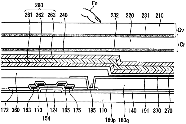
1. An organic light emitting device comprising:
a substrate;
a thin film transistor on a surface of the substrate;
a pixel electrode electrically connected to the thin film transistor;
a partition defining an opening on the pixel electrode;
an organic light emitting layer comprising a portion disposed in the opening;
a common electrode on the organic light emitting layer and the partition;
at least two encapsulation layers formed on the common electrode to encapsulate an organic light emitting element comprising the pixel electrode, the organic light emitting layer, and the common electrode, the at least two encapsulation layers comprising at least one inorganic layer comprising a first portion overlapping the opening and a second portion overlapping the partition without the opening and adjacent to the first portion in a plan view, the at least one inorganic layer comprising silicon nitride or silicon oxide;
a first planarization layer formed on the at least two encapsulation layers; and
a touch sensor formed on the first planarization layer without any adhesive layer for adhering between the touch sensor and the first planarization layer,
wherein:
a first distance between a first surface of the first portion and the surface of the substrate is less than a second distance between a second surface of the second portion and the surface of the substrate;
the touch sensor comprises a capacitive conductive layer; and
the first planarization layer is interposed between the touch sensor and the at least two encapsulation layers.
|