| CPC H10B 43/27 (2023.02) [H10B 43/50 (2023.02)] | 21 Claims |
|
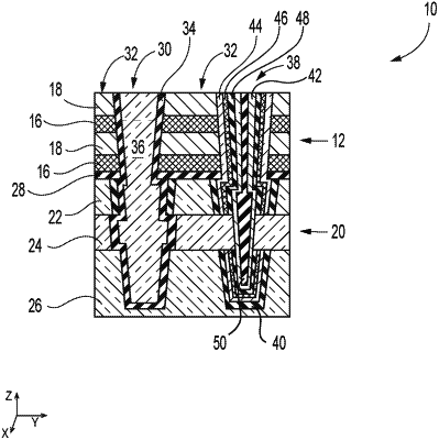
1. A microelectronic device, comprising:
a source structure comprising:
a source region;
a cap region vertically overlying the source region; and
a lateral contact region vertically interposed between the source region and the cap region;
a stack structure comprising a vertically alternating sequence of insulative structures and conductive structures;
filled slits extending through the stack structure and into the source structure, the filled slits dividing the stack structure into multiple blocks and each comprising:
a dielectric liner horizontally adjacent the stack structure and the source structure, portions of the dielectric liner within vertical boundaries of the lateral contact region of the source structure outwardly horizontally offset from additional portions of the dielectric liner within vertical boundaries of the source region and the cap region of the source structure; and
a fill material surrounded by the dielectric liner; and
memory cell pillars extending through the stack structure and into the source structure, the memory cell pillars and the filled slits terminating at substantially the same vertical position within the source structure as one another.
|