| CPC H05K 1/115 (2013.01) [G06F 1/189 (2013.01); H05K 2201/0338 (2013.01); H05K 2201/041 (2013.01)] | 14 Claims |
|
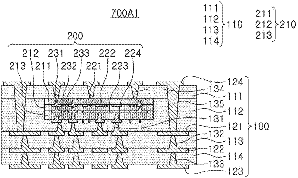
1. A substrate structure comprising:
a first printed circuit board including a plurality of first insulating layers and a plurality of first wiring layers, respectively disposed on or between the plurality of first insulating layers; and
a connection structure disposed in the first printed circuit board and including a plurality of internal insulating layers and a plurality of internal wiring layers, respectively disposed on or between the plurality of internal insulating layers,
wherein a first one of the plurality of first insulating layers is in contact with one surface of the connection structure, and a second one of the plurality of first insulating layers is in contact with another surface of the connection structure opposing the one surface and extends to cover a side surface of the connection structure,
a first via disposed in the first one of the plurality of first insulating layers to connect to one of the plurality of internal wiring layers, and a second via disposed in the second one of the plurality of first insulating layers and extending from another of the plurality of internal wiring layers to one of the plurality of first wiring layers are tapered in opposing directions, and
a third via is disposed in a third one of the plurality of first insulating layers and extends from the one of the plurality of first wiring layers to another of the plurality of first wiring layers.
|