| CPC H05K 1/113 (2013.01) [H05K 2201/096 (2013.01); H05K 2201/09827 (2013.01)] | 20 Claims |
|
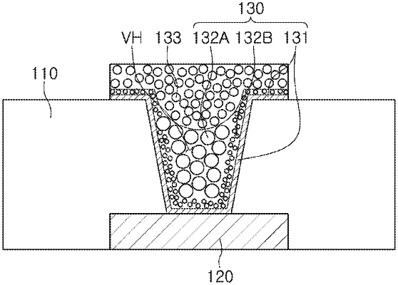
1. A printed circuit board, comprising: an insulating layer; a metal pad disposed on one side of the insulating layer; a via hole penetrating through the insulating layer to expose at least a portion of the metal pad; and a via filling at least a portion of the via hole, wherein the via comprises a first metal layer, a second metal layer directly disposed on a top of the first metal layer, and a third metal layer directly disposed on the second metal
layer, wherein the first metal layer, the second metal layer, and the third metal layer are arranged upwardly from the metal pad in the listed order, and an average size of grains in the second metal layer is larger than an average size of grains in the third metal layer.
|