| CPC H05K 1/0225 (2013.01) [B60R 16/03 (2013.01); H05K 1/18 (2013.01); H05K 9/0064 (2013.01); H01R 12/75 (2013.01); H01R 2201/04 (2013.01); H01R 2201/26 (2013.01); H05K 2201/0715 (2013.01); H05K 2201/0723 (2013.01); H05K 2201/10189 (2013.01)] | 21 Claims |
|
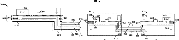
1. A printed circuit board comprising:
a substrate defining a major plane;
a first side of the major plane of the substrate configured for mounting thereon of functional circuit elements;
a cable connector mounted on a second side of the major plane of the substrate, opposite the first side, for coupling to a shielded radiofrequency (RF) communications cable;
at least one component grounding layer parallel to the major plane configured for coupling to the functional elements; and
at least one cable grounding layer parallel to the major plane and separated from the at least one component grounding layer, each cable grounding layer in the at least one cable grounding layer being coextensive with the full expanse of the substrate and being configured for coupling, through the connector, to shielding of the shielded RF communications cable, without coupling to any other component.
|