| CPC H04N 25/778 (2023.01) [H03F 3/16 (2013.01); H01L 31/03046 (2013.01); H03F 2200/144 (2013.01)] | 12 Claims |
|
1. A solid-state imaging device comprising:
a plurality of pixel units; a correction unit; and a control unit, wherein
each of the plurality of pixel units includes:
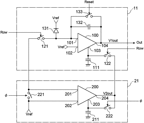
a main amplifier having a first input terminal, a second input terminal, a third input terminal, and an output terminal, and configured to output, from the output terminal, a voltage value according to a sum of a product of a first gain and a potential difference of the first input terminal with respect to the second input terminal and a product of a second gain and a potential difference of the third input terminal with respect to the second input terminal;
a capacitive element connected to the third input terminal of the main amplifier;
a first switch connected to the first input terminal of the main amplifier;
a second switch connected to the third input terminal of the main amplifier;
a photodiode connected to the first input terminal of the main amplifier;
a feedback capacitive element provided between the first input terminal and the output terminal of the main amplifier, and configured to accumulate a charge generated in the photodiode in response to light incidence; and
an initialization switch provided in parallel with the feedback capacitive element,
the correction unit includes:
a null amplifier having a first input terminal, a second input terminal, a third input terminal, and an output terminal, the first input terminal being connected to the first switch of each of the plurality of pixel units, the output terminal being connected to the second switch of each of the plurality of pixel units, and configured to output, from the output terminal, a voltage value according to a difference between a product of a first gain and a potential difference of the first input terminal with respect to the second input terminal and a product of a second gain and a potential difference of the third input terminal with respect to the second input terminal;
a capacitive element connected to the third input terminal of the null amplifier;
a first switch provided between the first input terminal and the second input terminal of the null amplifier; and
a second switch provided between the third input terminal and the output terminal of the null amplifier, and
the control unit is configured to:
perform initialization and charge accumulation of the feedback capacitive element by controlling ON/OFF of the initialization switch for each of the plurality of pixel units,
set the first switch and the second switch to an ON state sequentially for each of the plurality of pixel units, and
set the first switch and the second switch of the correction unit to the ON state in a period in which the first switches and the second switches of all of the plurality of pixel units are set to an OFF state.
|