| CPC H04N 25/709 (2023.01) [H04N 25/707 (2023.01); H04N 25/766 (2023.01)] | 4 Claims |
|
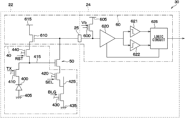
1. A solid-state imaging element comprising:
a pixel including
a photoelectric conversion element configured to generate, by photoelectric conversion, a photocurrent corresponding to an amount of light,
a charge accumulation unit configured to
accumulate a charge corresponding to the photocurrent, and
output a voltage corresponding to an amount of the charge accumulated in the charge accumulation unit,
a power supply,
a transistor configured to be connected to the power supply,
a drive circuit configured to apply a voltage to the transistor to turn on the transistor,
a common transistor having a first terminal and a second terminal, the common transistor configured to
maintain a voltage of the first terminal at a predetermined voltage with a voltage applied from the power supply and output a voltage corresponding to a change in the voltage of the charge accumulation unit from the second terminal, based on a condition that an element voltage as the voltage applied from the drive circuit to the transistor is a ground voltage,
output a voltage corresponding to a change in the voltage of the charge accumulation unit from the first terminal, based on a condition that the element voltage is higher than the ground voltage, and
a detection unit configured to detect whether the voltage from the first terminal of the common transistor has increased or decreased; and
an image processing unit configured to generate a luminance image based on a change in the voltage output from the second terminal of the common transistor, based on a condition that the element voltage is the ground voltage.
|