| CPC H04B 7/0413 (2013.01) [H01Q 3/267 (2013.01); H01Q 21/0006 (2013.01); H01Q 21/065 (2013.01); H01Q 21/29 (2013.01); H01Q 25/001 (2013.01); H01Q 1/02 (2013.01); H01Q 1/42 (2013.01); H01R 12/73 (2013.01)] | 20 Claims |
|
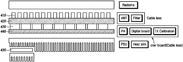
1. A multiple-input multiple-output (MIMO) antenna system comprising:
a radome;
a housing including a heat sink on a rear side thereof; and
an antenna assembly having a stacked structure and embedded between the radome and the housing,
wherein the antenna assembly comprises:
a first printed circuit board (PCB) on which a feeding network is provided;
a plurality of antenna elements provided on an upper surface of the first PCB,
and electrically connected to the feeding network;
a second PCB arranged under the first PCB, the second PCB including:
a plurality of transmitting and receiving circuits; and
a digital circuit being configured to perform digital processing on a baseband signal and electrically connected to the plurality of transmitting and receiving circuits; and
a filter assembly disposed between the first PCB and the second PCB, the filter assembly including the plurality of band-pass filters which are assembled in a line on a push bar,
wherein a filter body of each of the plurality of band-pass filters is attached to the first PCB, and a first port of each of the plurality of band-pass filters is directly connected to the feeding network without radio-frequency (RF) cabling, and
wherein, when the push bar is fastened to the second PCB, a second port of each of the plurality of band-pass filters is directly connected to one of the transmitting and receiving circuits without RF cabling.
|