| CPC H03L 7/0807 (2013.01) [H03K 3/037 (2013.01); H03L 7/0893 (2013.01); H03L 7/091 (2013.01); H03L 7/0992 (2013.01); H03L 7/0995 (2013.01); H03L 7/189 (2013.01); H03M 1/38 (2013.01)] | 19 Claims |
|
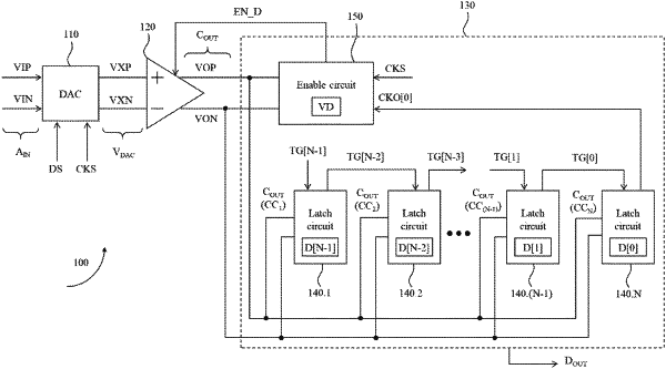
1. A successive-approximation register (SAR) analog-to-digital converter (ADC) circuit, comprising:
a comparator circuit, configured to compare an analog signal with a plurality of reference levels; and
a plurality of latch circuits, coupled to the comparator circuit and connected in series, the latch circuits being triggered sequentially in response to a plurality of trigger signals, respectively, to store a comparator output of the comparator circuit and accordingly generate a digital signal, wherein a first latch circuit and a second latch circuit of the latch circuits are triggered in response to a first trigger signal and a second trigger signal of the trigger signals, respectively; the first latch circuit is configured to generate the second trigger signal according to the comparator output stored in the first latch circuit wherein the first latch circuit comprises: a data latch configured to, when triggered in response to the first trigger signal, store the comparator output to generate a data signal; a signal detector, coupled to the data latch, the signal detector being configured to detect the data signal to generate a first valid signal indicating if the data signal is valid; and a delay element, coupled to the signal detector, the delay element being configured to delay the first valid signal to generate the second trigger signal.
|