| CPC H03K 17/6872 (2013.01) [H04B 1/40 (2013.01)] | 17 Claims |
|
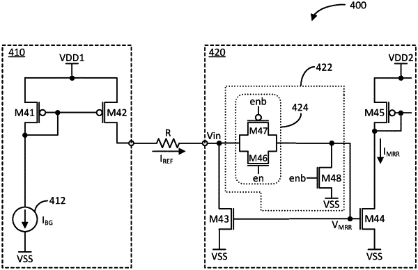
1. An integrated circuit (IC), comprising:
a current mirror, comprising:
a first field effect transistor (FET) including a first drain, a first gate, and a first source, wherein the first source is coupled to a first voltage rail; and
a second FET including a second drain, a second gate, and a second source, wherein the second gate is coupled to the first gate of the first FET, and the second source is coupled to the first voltage rail; and
a selective coupling circuit configured to selectively couple the first drain of the first FET to the first and second gates of the first and second FETs based on a voltage at the first drain of the first FET, wherein the selective coupling circuit comprises
a third FET including a third source, a third gate, and a third drain, wherein the third source is coupled to the first drain of the first FET, and
an inverter coupled between the first drain of the first FET and the first voltage rail, wherein the inverter includes an input coupled to the third drain of the third FET, and an output coupled to the third gate of the third FET.
|