US 11,736,090 B2
Film bulk acoustic resonators in thin LN-LT layers
Viktor Plesski, Gorgier (CH); and Julius Koskela, Helsinki (FI)
Assigned to Murata Manufacturing Co., Ltd., Nagaokakyo (JP)
Filed by Murata Manufacturing Co., Ltd., Nagaokakyo (JP)
Filed on Oct. 29, 2021, as Appl. No. 17/515,333.
Application 17/515,333 is a continuation of application No. 17/125,779, filed on Dec. 17, 2020, granted, now 11,251,775.
Application 17/125,779 is a continuation of application No. 17/090,599, filed on Nov. 5, 2020, granted, now 10,944,380, issued on Mar. 9, 2021.
Application 17/090,599 is a continuation of application No. 16/932,719, filed on Jul. 18, 2020, granted, now 10,862,454, issued on Dec. 8, 2020.
Claims priority of provisional application 62/958,851, filed on Jan. 9, 2020.
Claims priority of provisional application 62/875,855, filed on Jul. 18, 2019.
Prior Publication US 2022/0407498 A1, Dec. 22, 2022
This patent is subject to a terminal disclaimer.
Int. Cl. H03H 9/205 (2006.01); H03H 9/56 (2006.01); H03H 9/02 (2006.01); H03H 9/13 (2006.01)
CPC H03H 9/205 (2013.01) [H03H 9/0211 (2013.01); H03H 9/02015 (2013.01); H03H 9/131 (2013.01); H03H 9/564 (2013.01)] 20 Claims
OG exemplary drawing
 
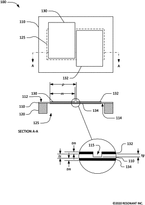
1. An acoustic resonator device comprising:
a piezoelectric plate having a front surface and a back surface opposite the front surface;
a back-side conductor pattern formed on the back surface; and
a first front-side conductor pattern and a second front-side conductor pattern formed on respective portions of the front surface opposite the back-side conductor pattern, wherein a portion of the piezoelectric plate between the first front-side conductor pattern and the back-side conductor pattern forms a first resonator and a portion of the piezoelectric plate between the second front-side conductor pattern and the back-side conductor pattern forms a second resonator.