| CPC H02M 3/335 (2013.01) [H02M 1/143 (2013.01); H02M 1/32 (2013.01); H02M 3/33569 (2013.01); H02M 7/003 (2013.01)] | 11 Claims |
|
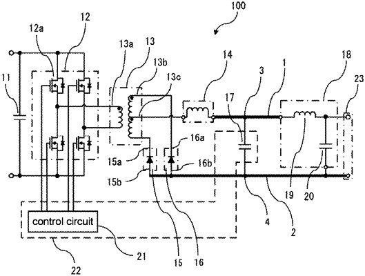
1. A power conversion device comprising:
a base;
a transformer disposed on a first surface of the base and having a primary winding and a secondary winding;
an inverter portion having a semiconductor switching element and configured to supply power to the primary winding;
a control substrate disposed apart from the first surface of the base and having a control circuit configured to control the inverter portion;
a first rectification element having a first terminal which is connected to one end portion of the secondary winding and which is provided adjacent to the transformer, the first rectification element further having a second terminal, the first rectification element being disposed on a first surface side of the base so as to be located on a specific direction side relative to the transformer;
a second rectification element having a third terminal which is connected to another end portion of the secondary winding and which is provided adjacent to the transformer, the second rectification element further having a fourth terminal, the second rectification element being disposed, side by side with the first rectification element, on the first surface side of the base so as to be located on the specific direction side relative to the transformer;
a smoothing reactor disposed on the first surface of the base and having one end portion connected to a center tap which is provided between the one end portion and the other end portion of the secondary winding;
an output filter circuit portion connected between another end portion of the smoothing reactor and a high-potential side of an external load;
a first main circuit wire making connection between the other end portion of the smoothing reactor and the output filter circuit portion;
a second main circuit wire making connection between a low-potential side of the external load and each of the second terminal of the first rectification element and the fourth terminal of the second rectification element; and
a plurality of smoothing capacitors, each having a high-potential-side terminal connected to the first main circuit wire, and each having a low-potential-side terminal connected to the second main circuit wire, said plurality of smoothing capacitors each being mounted on the control substrate, wherein
in a plan view of the control substrate, a subset of said plurality of smoothing capacitors and a target region obtained by combining a region in which the first rectification element is disposed, a region in which the second rectification element is disposed, and a region between the first rectification element and the second rectification element, overlap with each other, and
in said plan view, of the control substrate, a low-potential-side connection point of each of the plurality of smoothing capacitors, connected to the second main circuit wire, is disposed so as to overlap with the control substrate and a region obtained by extending the target region in the specific direction and a direction opposite to the specific direction.
|