| CPC H02H 7/1213 (2013.01) [H02M 3/003 (2021.05); H02M 3/335 (2013.01)] | 22 Claims |
|
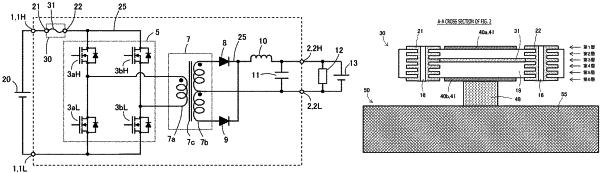
1. A power converter comprising:
a semiconductor element;
a breaking mechanism that breaks current when excessive current flows; and
a wiring member that connects the semiconductor element and the breaking mechanism,
wherein the breaking mechanism is provided with
a multilayer circuit board in which a plurality of conductive patterns including a fuse pattern which fuses when excessive current flows and a plurality of insulating members are laminated, and
a support member which is provided with a support body part; a fixation projection part which projected from the support body part to the multilayer circuit board side and to which the multilayer circuit board was fixed; and a support projection part which projected from the support body part to the multilayer circuit board side and supports an one side circuit board face of the multilayer circuit board,
wherein the fuse pattern is provided in an inner layer of the multilayer circuit board, and
wherein the support projection part overlaps with at least one part of a fusing part of the fuse pattern, viewing in a normal direction of the circuit board face of the multilayer circuit board.
|