| CPC H01Q 1/2283 (2013.01) [H01L 23/49838 (2013.01); H01L 23/66 (2013.01); H01Q 1/3233 (2013.01); H01Q 1/50 (2013.01); H01Q 1/525 (2013.01); H01Q 13/02 (2013.01); H01Q 21/0006 (2013.01); H01L 2223/6627 (2013.01); H01L 2223/6677 (2013.01)] | 29 Claims |
|
1. A high frequency wireless device, comprising:
a printed circuit board (PCB);
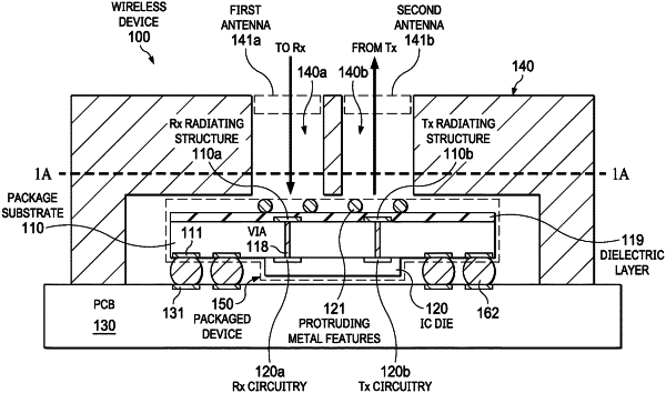
a three-dimensional (3D) antenna structure mounted on a top surface of the PCB including a first antenna connected to a first waveguide feed and a second antenna connected to a second waveguide feed;
a packaged device comprising a package substrate attached to the top surface of the PCB having a top metal surface including a transmit (Tx) radiating structure under the second waveguide feed and a receive (Rx) radiating structure under the first waveguide feed, with a radio frequency (RF) connection from the top metal surface to a bottom surface, with an integrated circuit (IC) die flipchip attached to the bottom surface that includes at least one Rx channel including Rx circuitry and at least one Tx channel comprising Tx circuitry, and with the Rx and Tx channels connected by respective ones of the RF connection to the Tx radiating structures and to the Rx radiating structures;
a dielectric layer on the top metal surface;
at least one row of protruding metal features on the dielectric layer positioned under the first and second waveguide feeds on at least 2 sides of the Tx radiating structure and the Rx radiating structure configured to create a waveguiding wall structure for directing signals from the Tx radiating structure through the second waveguide feed to the second antenna from the first antenna through the first waveguide feed to the Rx radiating structure.
|