| CPC H01L 33/62 (2013.01) [F21S 4/24 (2016.01); F21S 43/14 (2018.01); H01L 22/12 (2013.01); H01L 25/0753 (2013.01); H01L 2933/0066 (2013.01)] | 17 Claims |

|
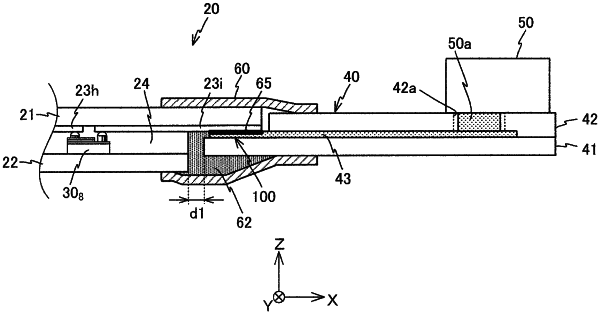
1. A light emitting device comprising:
a light emitting panel comprising:
a first substrate, which is flexible,
a plurality of conductor patterns, which are formed on a surface of the first substrate,
a plurality of light emitting elements, each of which is connected to at least two of the conductor patterns, and
a resin layer, which holds the light emitting elements on the first substrate;
a wiring substrate comprising:
an insulating base, and
a circuit pattern that is formed on the insulating base and electrically connected with an exposed part of the conductor patterns that is exposed from an end part of the resin layer; and
a mold resin, which covers part of the conductor patterns and part of the circuit pattern, and which covers the end part of the resin layer and an end part of the insulating base.
|