| CPC H01L 33/60 (2013.01) [H01L 33/505 (2013.01); H01L 33/507 (2013.01); H01L 33/58 (2013.01); H01L 33/62 (2013.01); H01L 25/0753 (2013.01); H01L 33/44 (2013.01); H01L 33/54 (2013.01); H01L 33/56 (2013.01); H01L 2224/05001 (2013.01); H01L 2224/05023 (2013.01); H01L 2224/0568 (2013.01); H01L 2224/05568 (2013.01); H01L 2224/05644 (2013.01); H01L 2224/05655 (2013.01); H01L 2224/05664 (2013.01); H01L 2224/05666 (2013.01); H01L 2224/05669 (2013.01); H01L 2224/05671 (2013.01); H01L 2224/05673 (2013.01); H01L 2224/05684 (2013.01); H01L 2224/14 (2013.01); H01L 2224/16225 (2013.01); H01L 2224/73253 (2013.01); H01L 2924/013 (2013.01); H01L 2933/0091 (2013.01)] | 21 Claims |
|
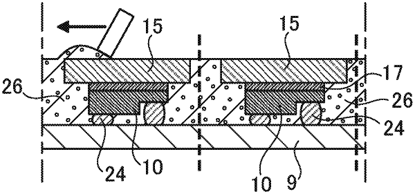
1. A method for producing a plurality of light emitting apparatuses, the method comprising:
mounting a plurality of light emitting devices on a collective wiring substrate such that the plurality of light emitting devices are electrically connected to the collective wiring substrate, wherein each light emitting device has a mount surface at which the light emitting device is mounted to the collective wiring substrate, and a light outgoing surface opposite the mount surface;
attaching a plurality of light transparent members to the light outgoing surfaces of the light emitting devices such that each light transparent member is attached to the light outgoing surfaces of one or more of the light emitting devices;
forming a collective covering member that covers at least lateral surfaces of the light transparent members and lateral surfaces of the plurality of light emitting devices such that a light emission surface of each light transparent member is exposed from the collective covering member, wherein the collective covering member comprises a resin and a light reflective material; and
cutting the collective covering member and the collective wiring substrate without cutting the light transparent members so as to form the plurality of light emitting apparatuses, each comprising a wiring substrate formed from the collective wiring substrate, said one or more of the light emitting devices mounted on the wiring substrate, one of the light transparent members that receives incident light emitted from said one or more of the light emitting devices, and a covering member formed from the collective covering member.
|