| CPC H01L 33/0095 (2013.01) [H01L 33/007 (2013.01); H01L 33/22 (2013.01); H01L 33/507 (2013.01); H01L 2933/0041 (2013.01)] | 14 Claims |
|
1. A method for manufacturing a light-emitting element, the method comprising:
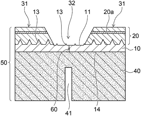
forming a semiconductor structure comprising a light-emitting layer on a first surface of a substrate, wherein the first surface comprises a plurality of protrusions;
dividing the semiconductor structure into a plurality of light-emitting portions by removing a portion of the semiconductor structure so as to form an exposed region of the substrate, wherein the first surface is exposed from under the semiconductor structure in the exposed region;
etching the protrusions formed in the exposed region;
bonding a light-transmitting body to a second surface of the substrate that is opposite the first surface so as to form a bonded body, wherein the light-transmitting body comprises a fluorescer;
after the step of bonding the light-transmitting body to the second surface, forming a plurality of modified regions along the exposed region inside the substrate by irradiating a laser beam on the exposed region from a first surface side;
after the step of forming the plurality of modified regions, removing a portion of the light-transmitting body that overlaps the plurality of modified regions in a plan view; and
singulating the bonded body along the modified regions.
|