| CPC H01L 29/78642 (2013.01) [H01L 27/1203 (2013.01); H01L 27/13 (2013.01); H10B 12/05 (2023.02); H10B 12/31 (2023.02); H10B 53/20 (2023.02)] | 11 Claims |
|
1. An integrated transistor, comprising:
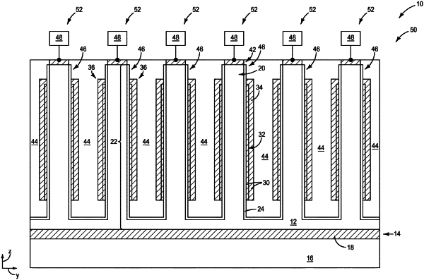
an active region pillar over a base, the active region pillar comprising semiconductor material having opposing sidewalls;
an insulative material against an entirety of the opposing sidewalls of the active region pillar and extending over the base adjacent the active region pillar;
an insulative step along the insulative material proximate a bottom portion of the active region pillar; and
a conductive gating structure operatively proximate the active region and spaced from the base by the insulative material and the insulative step;
the conductive gating structure including an inner region proximal the active region and including an outer region distal from the active region; the inner region comprising a first material which includes titanium and nitrogen, and the outer region comprising a metal-containing second material; the second material having a higher conductivity than the first material and being present along an entirety of an outer surface and at least a portion of an upper surface of the inner region.
|