| CPC H01L 29/7856 (2013.01) [H01L 29/6653 (2013.01); H01L 29/66803 (2013.01); H01L 29/7783 (2013.01); H01L 29/7788 (2013.01)] | 12 Claims |
|
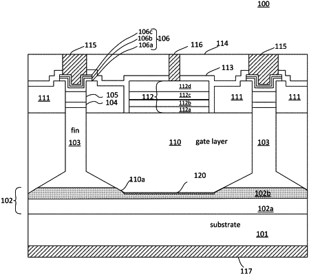
1. A method of fabricating a vertical fin-based field effect transistor (FET), the method comprising:
providing a semiconductor substrate having a first surface and a second surface, the semiconductor substrate having a first conductivity type;
epitaxially growing a first semiconductor layer on the first surface of the semiconductor substrate, the first semiconductor layer having the first conductivity type and including a drift layer and a graded doping layer on the drift layer;
epitaxially growing a second semiconductor layer having the first conductivity type on the graded doping layer;
forming a metal compound layer on the second semiconductor layer;
forming a patterned hard mask layer on the metal compound layer;
etching the metal compound layer and the second semiconductor layer using the patterned hard mask layer as a mask exposing a surface of the graded doping layer to form a plurality of fins surrounded by a trench; and
terminating the etching in the graded doping layer.
|