| CPC H01L 29/7827 (2013.01) [H01L 21/0262 (2013.01); H01L 21/02546 (2013.01); H01L 21/30621 (2013.01); H01L 29/0657 (2013.01); H01L 29/0847 (2013.01); H01L 29/1037 (2013.01); H01L 29/207 (2013.01); H01L 29/66522 (2013.01); H01L 29/66666 (2013.01)] | 20 Claims |
|
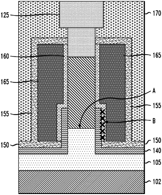
1. A semiconductor device, comprising:
at least one fin on a semiconductor substrate, the at least one fin comprising a channel layer stacked on top of a source layer and a drain layer stacked on top of the channel layer;
a cap layer disposed on a lower portion of the at least one fin comprising the source layer and part of the channel layer; and
a gate structure comprising a gate dielectric layer and a gate conductor disposed on the at least one fin and on the cap layer;
wherein the cap layer is positioned between the lower portion of the at least one fin and the gate dielectric layer; and
wherein the cap layer extends perpendicularly with respect to a top surface of the semiconductor substrate along a lateral side of the at least one fin to an uppermost height below the top of the channel layer;
wherein a first portion of the gate dielectric layer is disposed on a side of the cap layer, and a second portion of the gate dielectric layer is disposed on a part of the lateral side of the at least one fin without the cap layer positioned between the part of the lateral side of the at least one fin and the second portion of the gate dielectric layer; and
wherein the lattice constants of the cap layer, of the channel layer and of the source layer are the same.
|