| CPC H01L 29/1095 (2013.01) [H01L 29/0684 (2013.01); H01L 29/086 (2013.01); H01L 29/1608 (2013.01); H01L 29/66068 (2013.01); H01L 29/7397 (2013.01); H01L 29/7813 (2013.01); H01L 21/046 (2013.01)] | 3 Claims |
|
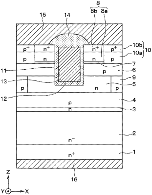
1. A manufacturing method of a silicon carbide semiconductor device including an inverted semiconductor element, the manufacturing method comprising:
preparing a substrate made of silicon carbide of a first or second conductivity type;
forming a drift layer made of silicon carbide of the first conductivity type and having an impurity concentration lower than an impurity concentration of the substrate above the substrate;
forming a base region made of silicon carbide of the second conductivity type above the drift layer;
forming a source region made of silicon carbide of the first conductivity type and having an impurity concentration higher than the impurity concentration of the drift layer above the base region;
forming a trench gate structure by providing, from a surface of the source region, a plurality of gate trenches deeper than the base region and aligned in stripes with one direction as a longitudinal direction, forming a gate insulating film on inner wall surfaces of the gate trenches, and forming a gate electrode on the gate insulating film;
forming a source electrode electrically connected to the source region;
forming a drain electrode to a rear surface of the substrate; and
forming a non-doped layer made of silicon carbide between the forming the base region and the forming the source region,
wherein
the forming the base region and the forming the source region are performed by epitaxial growth, and
the forming the source region includes forming a first source region of the first conductivity type above the base region by epitaxial growth, and forming a second source region of the first conductivity type above the first source region by epitaxial growth, the second source region having an impurity concentration higher than an impurity concentration of the first source region and brought into contact with the source electrode.
|