| CPC H01L 29/6684 (2013.01) [H01L 29/516 (2013.01)] | 19 Claims |
|
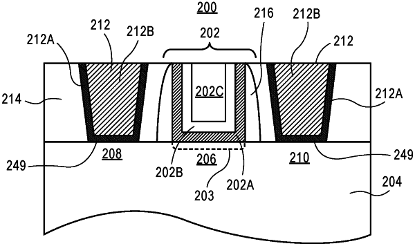
1. An integrated circuit structure, comprising:
a semiconductor channel structure comprising a monocrystalline material;
a gate dielectric over the semiconductor channel structure, the gate dielectric comprising a ferroelectric or antiferroelectric polycrystalline material layer, the ferroelectric or antiferroelectric polycrystalline material layer having an uppermost surface, and the gate dielectric further comprising an amorphous oxide layer between the ferroelectric or antiferroelectric polycrystalline material layer and the semiconductor channel structure, wherein the ferroelectric or antiferroelectric polycrystalline material layer is on and in direct contact with the amorphous oxide layer, and wherein the amorphous oxide layer is on and in direct contact with the semiconductor channel structure;
a gate electrode having a conductive layer on and in direct contact with the ferroelectric or antiferroelectric polycrystalline material layer, the conductive layer comprising a metal, and the conductive layer having an uppermost surface co-planar with the uppermost surface of the ferroelectric or antiferroelectric polycrystalline material layer, and the gate electrode having a gate fill layer on and in direct contact with the conductive layer;
a first source or drain structure at a first side of the gate electrode; and
a second source or drain structure at a second side of the gate electrode opposite the first side.
|