| CPC H01L 29/0847 (2013.01) [H01L 27/0886 (2013.01); H01L 29/0653 (2013.01); H01L 29/0673 (2013.01); H01L 29/785 (2013.01); H01L 29/7853 (2013.01)] | 21 Claims |

|
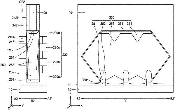
1. A semiconductor device comprising:
a substrate;
a plurality of channels on the substrate apart from one another in a vertical direction;
a gate structure contacting the plurality of channels;
a gate spacer on at least one side surface of the gate structure; and
a source/drain structure contacting the plurality of channels, the source/drain structure comprising one of a source structure and a drain structure,
wherein a topmost portion of a bottom surface of the gate spacer is lower than a topmost portion of a top surface of a topmost channel from among the plurality of channels,
a topmost portion of a top surface of the source/drain structure is lower than the topmost portion of the top surface of the topmost channel, and
wherein the topmost portion of the bottom surface of the gate spacer contacts the source/drain structure.
|