US 11,735,620 B2
Solid-state imaging device having optical black region, method of manufacturing the same, and electronic apparatus
Kazufumi Watanabe, Tokyo (JP); and Yasushi Maruyama, Kanagawa (JP)
Assigned to SONY GROUP CORPORATION, Tokyo (JP)
Filed by Sony Group Corporation, Tokyo (JP)
Filed on Dec. 29, 2021, as Appl. No. 17/564,666.
Application 14/563,036 is a division of application No. 12/699,488, filed on Feb. 3, 2010, granted, now 8,928,784, issued on Jan. 6, 2015.
Application 17/564,666 is a continuation of application No. 16/178,454, filed on Nov. 1, 2018, granted, now 11,264,423.
Application 16/178,454 is a continuation of application No. 15/647,093, filed on Jul. 11, 2017, granted, now 10,141,365, issued on Nov. 27, 2018.
Application 15/647,093 is a continuation of application No. 15/394,241, filed on Dec. 29, 2016, granted, now 9,799,698, issued on Oct. 24, 2017.
Application 15/394,241 is a continuation of application No. 14/942,691, filed on Nov. 16, 2015, granted, now 9,570,500, issued on Feb. 14, 2017.
Application 14/942,691 is a continuation of application No. 14/563,036, filed on Dec. 8, 2014, granted, now 9,647,025, issued on May 9, 2017.
Claims priority of application No. 2009-028822 (JP), filed on Feb. 10, 2009; and application No. 2009-148088 (JP), filed on Jun. 22, 2009.
Prior Publication US 2022/0123041 A1, Apr. 21, 2022
Int. Cl. H01L 27/146 (2006.01); H04N 25/62 (2023.01); H01L 31/0216 (2014.01); H01L 31/18 (2006.01); H01L 21/78 (2006.01)
CPC H01L 27/14645 (2013.01) [H01L 27/1463 (2013.01); H01L 27/1464 (2013.01); H01L 27/14612 (2013.01); H01L 27/14621 (2013.01); H01L 27/14623 (2013.01); H01L 27/14627 (2013.01); H01L 27/14629 (2013.01); H01L 27/14632 (2013.01); H01L 27/14636 (2013.01); H01L 27/14685 (2013.01); H01L 27/14687 (2013.01); H01L 31/0216 (2013.01); H01L 31/18 (2013.01); H04N 25/62 (2023.01); H01L 21/7806 (2013.01); H01L 31/02162 (2013.01); H01L 31/1804 (2013.01); Y02P 70/50 (2015.11)] 20 Claims
OG exemplary drawing
 
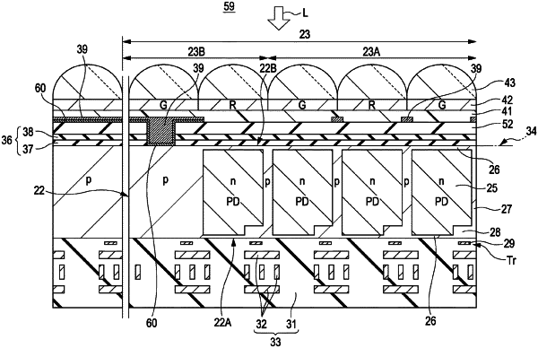
1. A light detecting device, comprising:
a semiconductor substrate including a first side as a light incident side and a second side opposite to the first side;
photoelectric conversion regions disposed in the semiconductor substrate;
an element isolation region disposed in the semiconductor substrate,
wherein the photoelectric conversion regions are separated by the element isolation region, and
wherein the element isolation region includes a p-type semiconductor region;
a wiring layer disposed under the second side of the semiconductor substrate; and
a metal film disposed above the first side of the semiconductor substrate,
wherein the metal film contacts the p-type semiconductor region in an optical black level region disposed in the semiconductor substrate.