| CPC H01L 27/14636 (2013.01) [H01L 27/1464 (2013.01); H01L 27/14618 (2013.01); H01L 27/14621 (2013.01); H01L 27/14627 (2013.01); H01L 27/14634 (2013.01); H01L 27/14645 (2013.01)] | 11 Claims |
|
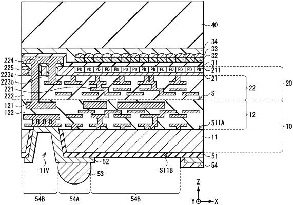
1. An imaging device comprising:
a photoelectric converter;
a protection member provided on a light incident side of the photoelectric converter;
a substrate opposed to the protection member with the photoelectric converter interposed therebetween and having a first surface on the photoelectric converter side and a second surface opposed to the first surface;
a rewiring layer provided in a selective region of the second surface of the substrate; and
a protective resin layer provided on the second surface of the substrate,
the second surface of the substrate having an external terminal coupling region exposed from the protective resin layer, and a stress relaxation region exposed from the protective resin layer and disposed at a position different from the external terminal coupling region, wherein the stress relaxation region is provided at a position not overlapping the rewiring layer.
|